The resources to understand the board are located
at
main megasquirtavr page
Look at the
- R38/R40 should be 1/2W , 1/4 Watt might fry!
You need to push it through the hole. Really. This will be fixed
in a new PCB revision, since the hole diameter and pad distance is not
optimal for 1/2 Watt resistor.
On the other hand the
BASE-EMITTER resistors of the big PNP (I used BD244) flyback
transistors can be 1/4 Watt (you have plenty of space there ;-).
- R1..4 can be 10k instead of 1k. There is no need to push 4mA
current into the BASE of a LED driving transistor. (Of course 1k works well,
don't change if you already installed).
I include one mail from Michael that is interesting for builders:
To: genboard@x-dsl.hu
Subject: Re: Sourceforge questions

> Is there a place that documents the correlation of software to hardware?

Not really. The time spent on writing documentation is close to zero. In the
schematic page 2, the subd37 connector layout, and the file global.h is
propably the best there is right now.

> Which FETs control which functions?

T1 and T2 are the injector drivers. T3 and T4 are the improved flyback. T8 is
the oldstyle backup flyback circuit.

> What do the header pins do?

Generally most headers on the board are for future usage. They aren't used
right now, but can be used for exiting add-on boards (more injector drivers,
ignition control, landing gear... whatever). Three of the headers are special:
ISP - for programming
J5 - must be connected for rs232 communication
J11 - tach circuit The rest can be used for whatever one likes.
This is basically a collection of replies to emails and general thoughts
related to components selection/assembly of the MegaSquirtAVR.
- Which AVR device?
ATmega128-16AI
The 16 is the speed (16 MHz), 'A' is the packaging, 'I' is for industrial
(-40C to 85C, then it also works in the winter).
- Zener diodes?
D4: It only handles negative voltages, I suggest using an 12V zener, but
anything smaller would work too. It shouldn't be larger since the voltage
regulator has -15V as minimum input voltage.
D5: The zener voltage must be higher than the peak battery voltage and lower
than the maximal input voltage to the voltage regulator. A zener around 20V -
22V is fine (14V < Vz < 26V).
D6 (mat), D8 (tps), D9 (clt):
If they are installed, they protect the AVR from getting fried
due to high voltage on the analog inputs. Unfortunately zeners aren't ideal
devices, so they will start conducting below 5.1v resulting in distortion of
the analog signals in the higher end of the scale (max voltage seen from the
ADC will be ~4.5V depending on the zener and series resistor).
Several solutions are available:
1) Don't install any zeners and hope the AVR's internal diodes can handle
overvoltage
2) Install 5v1 zeners thereby limiting the effective range of the ADC
3) Install 5v6 zeners to get some protection of the analog inputs and only
little interference with the analog signals
4) Install two BAT85 diodes on each analog signal. One of the diodes is
mounted where the zener was intended to be, and the other goes from the
analog signal to the little hole (Vref) near the edge (straight down) of the
pcb. This will protect the AVR and won't destroy the analog signal.
D7 (O2):
5v1 zener is fine
D11 (map):
Don't mount it if using onboard map sensor.
D13 (batt):
5v1 zener is fine
- Inductors?
Do either
1) Mount the two inductors. Suggested values L1 = 1uH, L2 = 10uH (was in the
drawer, works great).
2) Don't care about the inductors, the design works anyway. Use a small
resistor instead.
- Other important assembly notes
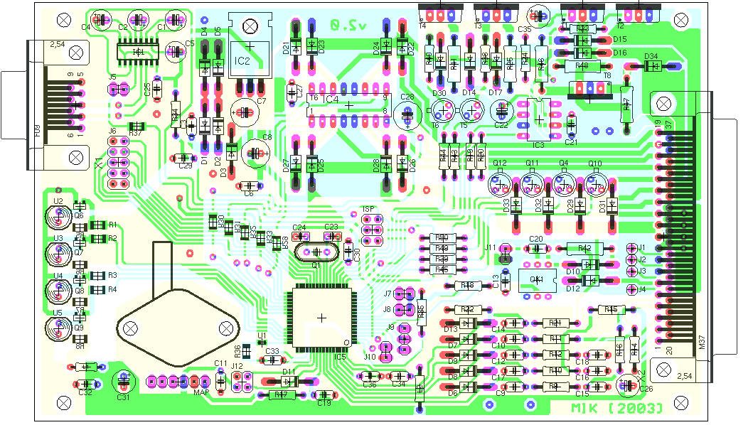
The via's under the subd-37 connector MUST be connected - all of them! They
are responsible for the ground connection to the entire pcb.
The crystal can be mounted on the bottom side, this eases soldering. Only do
this if you have a low (~3mm in height) one.
When using the MS, the "flyback return" should be connected to +12v. It can be
connected to ground instead, if the old flyback circuit is needed (with
replacement of some components).
Ground and analog ground must externally be separated. Analog ground is _only_
for sensors. It should not be connected to ground externally since this might
introduce a high current loop through the analog ground plane of the MS.
Be carefull with the Vref pin in the subd-37. If this accidentally is
connected to +12v you will a) call the fire department, b) have to start over
soldering a lot of components! (it is not a good idea either to connect it to
ground, so be carefull when mounting the tps sensor).
If you have some thermal conducting compound, it won't hurt using it under the
voltage regulator (LM2937, IC2) and a small 3mm screw to fixate it.
Don't mount the stepper driver (L293B, IC4) in a socket. The four middle pins
are transporting the heat to the butterfly shape surrounding the chip.
I have put a hex file for testing the megasquirt (the current code working in
my car) at http://caffrey.dk/megasquirt/files/megasquirt.hex.gz
If the board is assembled and the AVR is programmed correctly, then megatune
will happily communicate with the megasquirt.
a) A component soldered on both sides of the PCB won't fall off as easy as a
component soldered only on one side of the PCB.
b) There are placed some vias for tapping +5v, +12v, Vref and gnd around the
PCB. These are are not necessary to solder, all the others vias are! The way
to distinguish the two kinds of vias is simple: "if traces are going to the
via on both sides of the PCB, then it must be soldered/connected" - the same
must be done for components with both upper and lower connections.
what pin and function cmopatible device can be used to replace MC34151P ?
-
I'm using a TI UCC27323P on my daughter board, better specs
and half the price. [note: I haven't verified this.]
-
Other option is IXDI404PI
Please send updates to this page or other documentation to
cell at x-dsl.hu preferrably in html or diff form. Thanx.
If you really want to do the shopping, you can find the
list of components here (but you should verify it, and
always take the printed schematic and layout with you!)
BOM in compressed spreadsheet format
I suggest you are kind to yourself and buy a component kit from
Aaron
Most of the components are easy to get, but some needs to be ordered, and
it takes more time than ordering the complete kit.
genboard page